Chapter 2. The processor
27
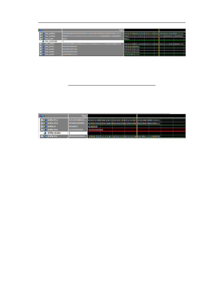
Figure 2.13: Mix Unit Simulation
Table 2.7: The Mix Unit ports
Name
Type
Size
Explanation
Rs1
input signal
64
Rs1 register data
Rs2
input signal
64
Rs2 register data
S
input signal
5
operation signals
enable
input signal
1
enable signal
Rd
output signal
64
Result data
Figure 2.14: Shifter Unit Simulation
2.5.4
The Shifter Unit
The shifter performs logic and arithmetic parallel shifts. The shifts can be either left or
right and the shift amount is determined by the instruction. The shifter consists of an
array of 8 barrel shifters. The formation is similar to that of the parallel adder since the
output bit of each 1byte shifter is redirected to the input of a specific shifter depending
on the subword size. The Shift unit is responsible for the shift instructions: Pshift,
Pshiftadd, Shrp, Slli, Srai, Srli. Table
displays all the ports used by the shifter unit.
Figure
displays an example simulation of the shifter where the pshift.l.8 instruction
is executed, where subwords of Rs1 are logically shifted to the left by Rs2 bits. The
maximum frequency is found from the propagation delay and is calculated to be 133,832
MHz. The occupied area is 1%.