Chapter 2. The processor
25
Figure 2.8: Carry out drive between two 64 bit numbers
Figure 2.9: Carry out drive between four 32 bit numbers
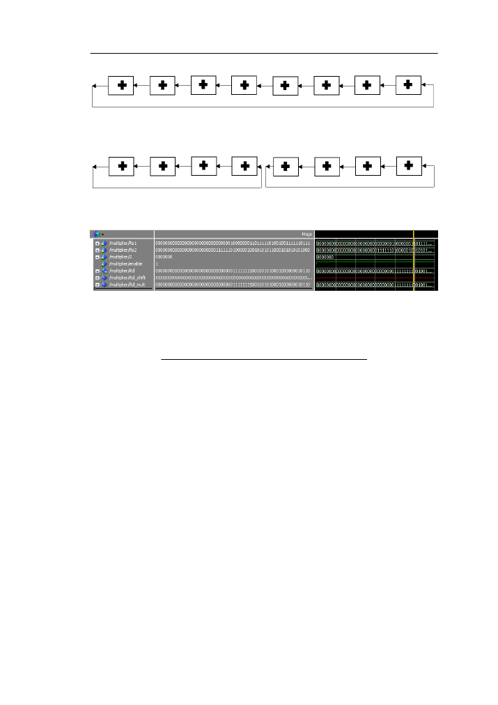
Figure 2.10: Multiplier Simulation
Table 2.6: The multiplier ports
Name
Type
Size
Explanation
Rs1
input signal
64
Rs1 register data
Rs2
input signal
64
Rs2 register data
S
input signal
7
operation signals
enable
input signal
1
enable signal
Rd
output signal
64
Result data
or even indexed subwords as shown in figures
and
. The two 32bit size products
of the multiplication form the new result. The multiplier performs the multiplication
instructions, which are the following: Pmul, Pmulshr. Table
displays the list of the
ports used by the multiplier module.
Figure
displays a simulation of the multiplier. The pmul.odd instruction is executed
where the odd indexed subwords(63 donwto 48 and 31 downto 16) of each of the values
in Rs1 and Rs2 are multiplied and the two 32 bit results are written to the left and right
half word respectively. Since the multiplier does not operate with a clock the maximum
frequency is calculated from the maximum propagation delay and is found to be 177,366
MHZ and it takes 1% of the FPGA area.