Chapter 2. The processor
19
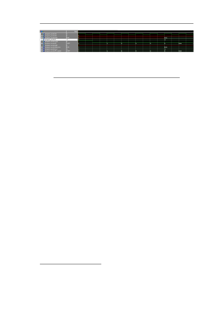
Figure 2.5: PC simulation
Table 2.1: Device Utilization Summary for the Program Counter
Logic Utilization
Used
Available
Utilization
Number of Slice Registers
64
93120
0%
Number of slice LUTs
134
46560
0%
Number of used LUT-FF pairs
64
134
47%
Number of bonded IOBs
156
240
65%
Number of BUFG/BUFGCTRLs
1
32
3%
default value added to the current PC to calculate the next address of the Instruction
Memory since the width of the memory is 32bits which is equal to the instruction word
size. As a result there is one instruction per line stored in the memory and the program
counter needs to increment by one to point to the next instruction. Some instructions
require the program counter to increment by a certain value; this value can be stored
either in the specified register Rd or it can be acquired directly from the instruction
stored in the instruction memory (input Imm). The width size of the program counter
value is 9 bits since the instruction memory size is 512 words. The value of the program
counter is reset either by an external signal or if the value reaches 512.
After the design of the module, it needs to be verified for proper functioning. The
program ”Modelsim PE student edition” was used to simulate the design and test the
correct functionality. In figure
a short simulation is displayed where the counter
increases for 5 cycles and in the sixth a constant value is added via the ”Imm” value.
2.3.2
Program Counter Metric Statistics
The maximum achieved frequency is 294.638MHz
. The size of this module is very small
since it only consists of a 64bit adder, a 64bit register and 3 multiplexers. Table
shows the device utilization summary as generated by the ISE development kit. The
total power consumption is 1.293Watts.
1
The device used for the implementation is the Xilinx Virtex ML605; more details provided in Chapter
6