Chapter 2. The processor
22
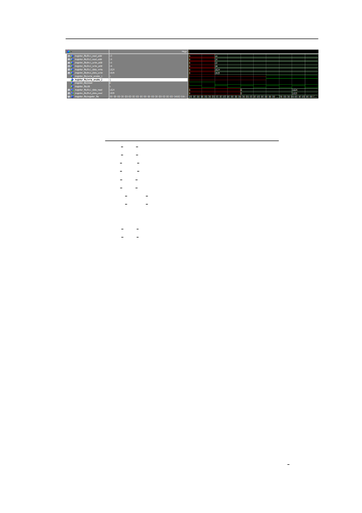
Figure 2.6: Register File Simulation
Table 2.4: The Register File Ports
Name
Type
Size
Explanation
Rs1 read addr
input signal
5
read address
Rs2 read addr
input signal
5
read address
Rs1 write addr
input signal
5
write address
Rs2 write addr
input signal
5
write address
Rs1 data write
input signal
64
write data
Rs2 data write
input signal
64
write data
write enable 1
input signal
1
write enable
write enable 2
input signal
1
write enable
reset
input signal
1
reset
clk
input signal
1
clock signal
Rs1 data read
output signal
64
data read output
Rs2 data read
output signal
64
data read output
the read ports do not register any change until the write enable signals are activated.
As soon as the write enable signals are activated the data read ports provide the value
in the next clock cycle. The register file operates at a maximum frequency of 382,117
MHz and occupies less than 1% of the FPGA
2.5
The third pipeline stage
The third stage of the pipeline is the data processing stage. Here all the data processing
takes place and all the data processing units are contained. This stage is the most time
consuming since it contains the slowest unit which is the shifter. This stage also contains
the predicate file and a sign extension unit along with some multiplexers.
2.5.1
The Arithmetic Logic Unit(ALU)
The ALU is responsible for the basic calculations(add, subtract), the comparisons and
the logic calculations. The top level design contains two components, the adder and the
logic calculations module as well as some logic for the calculation of the test bit. Table