RESEARCH POSTER PRESENTATION DESIGN © 2012
www.PosterPresentations.com
Reconfigurable hardware are becoming more popular in implementations where
flexibility, low cost and fast time to market are becoming essential attributes. The
use of soft microprocessors, along with the easy to use and flexible IP cores has
given rise to a need for an easy methodology and procedure to customize the soft
core designs. In this paper we present an example of the complete design and
customizing procedure of a soft microprocessor, implemented on FPGA. The
complete work flow is presented from designing the RTL and programming the
processor as long as the creation of the module to be embedded, in this case a low
cost, area-reduction oriented double precision FPU.
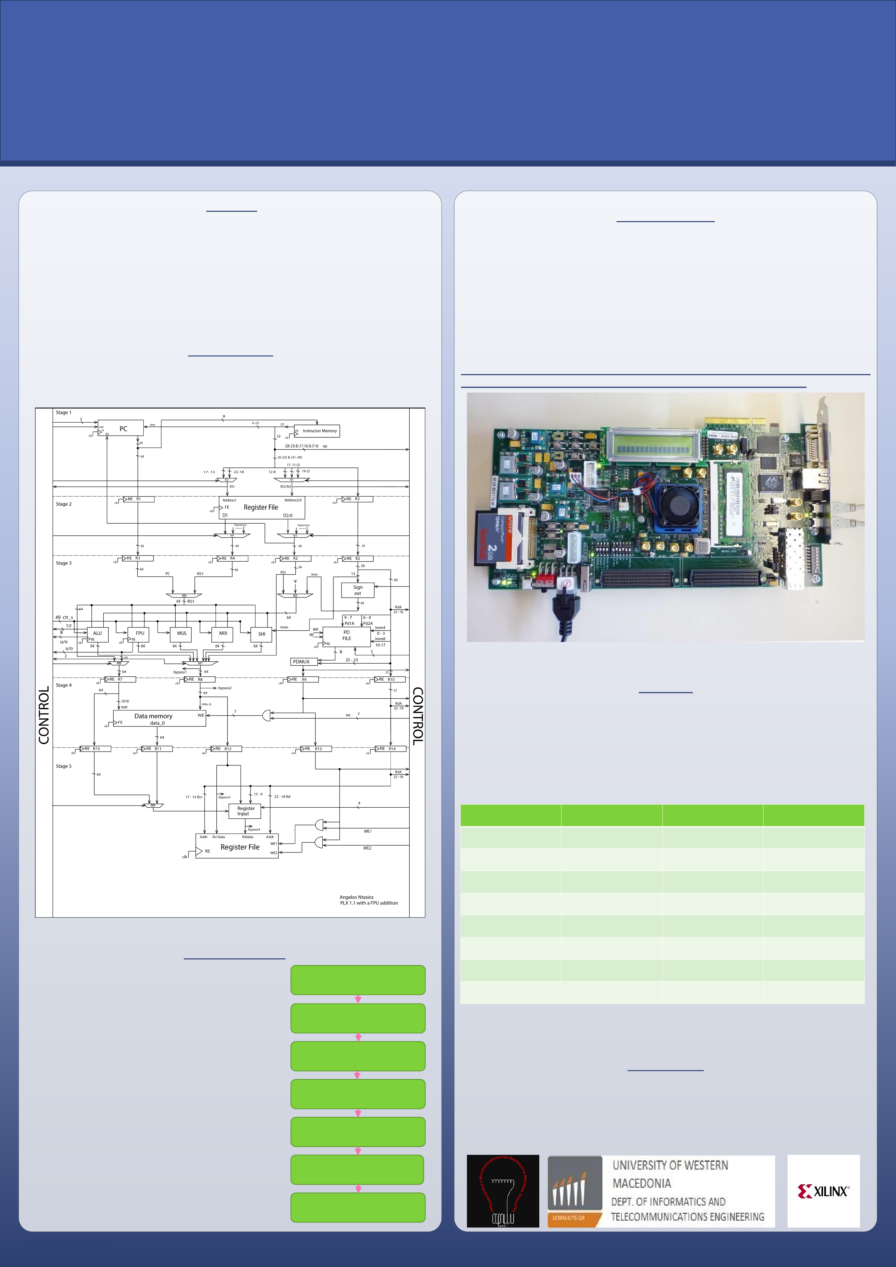
The instruction set that was implemented is the PLX 1.1, an ISA that focuses in
subword paralellism and is intended for multimedia processing. The following
figure(fig. 1) is the RTL schematic that implements the PLX 1.1 ISA.
Abstract
Implementetion
For the hardware implementation, we used a Xilinx Virtex 6 ML605 board. Synthesis
was performed by Xilinx ISE 14.3. and simulations using, “Modelsim PE Student edition
10.2C”. All synthesis designs were optimized for timing performance. Table I shows
the timing analysis, power consumption and area occupation for each module
individually. For the instruction memory and data memory the on board DDR3 memory
was used utilizing the interface provided by Xilinx, the IP Core Generator [6]. Two
block memories were generated with a maximum frequency 144MHZ. Table III displays
the maximum frequency and the required operation cycles. The power consumption is
3,422 Watt, as reported by the Xilinx Tools.
The maximum achieved frequency for the processor in the specific board is
58,289 MHz and the calculated Instructions Per Second 52955260 IPS.
Department of Informatics and Telecommunications, University of Western Macedonia
Angelos-Efstathios Ntasios Dr. Minas Dasygenis
Design and Implementation of a soft processor with
an embedded FPU
To create the IP block in the most efficient way, a
design flow has to be followed. In Figure 2 we
illustrate the fundamental steps of our design flow.
This design flow consists of seven steps. The first
step is to chose the Instruction Set Architecture
(ISA) of the processor to be implemented. The
second step is to create the processor RTL, which
provides an abstract view of the data flow and
functioning of the module. In the third step, we
describe the processor using an HDL and then select
an existing IP module or if it is not available we
create one. The next step is to verify the
functionality of the acquired or created module.
After the verification we need to customize the
existing ISA to support the new instructions that are
required for the new module to operate, which is
done in the fifth step. The next step is to customize
and create the proper wiring in the processor in
order to connect the new module, and the final
step is to test and verify the proper functionality of
the new design and fix any bugs discovered.
The processor
Future Work
Figure 1. The Processor RTL Schematic
ISA Specifications choice
Processor RTL Creation
Module Choice/Creation
Module Verification
ISA Customisation
Processor Customisation
Testing
The Xilinx Virtex 6 ML605 FPGA Board that was used for the implementation
Statistics
Optimization can be achieved in many different levels, area reduction, speed and
power optimization. However certain trade offs should be taken into consideration,
since all these attributes are dependent on each other. In our case the addition of the
FPU, being optimized for area reduction, has led to an approximate speed reduction
of the processor by about 30%. It is clear that many choices can be made in order to
achieve a golden mean in one’s design. Table I shows the basic metric statistics for all
the major components of the design.
Top Module
Max. Frequency
Operation Cycles
Area
Program Counter
58,289MHz
-
9% LUT slices
Register File
294,638 MHz
1
<1% LUT slices
ALU
382,117 MHz
1
4% LUT slices
FPU
218,627 MHz
1/2/3/4
1% LUT slices
MUL*
81,155 MHz
1/2/3/55
<1% LUT slices
MIX*
177,366 MHz
*
1% LUT slices
Shifter*
268,759 MHz
*
1% LUT slices
Top Module
133,832 MHz
*
1% LUT slices
Table I. Timing and area statistics
*These
modules
are
combinational
circuits and the maximum frequency has
been
calculated
by
the
maximum
propagation delay.
The Design FLow
• Further increase flexibility by creating a “self-adapted” processor to new modules.
• Creation of a Web-based platform to customise and create soft modules at will.
• Implement and customise new and more popular processors such as Picoblaze,
Microblaze etc.